Addressing the Vapor Distribution Challenge in PVT Crystal Growth Furnaces
Physical Vapor Transport (PVT) crystal growth remains one of the most technically demanding processes in third-generation semiconductor manufacturing. Within these high-temperature thermal fields, non-uniform gas distribution and impurity contamination are persistent obstacles that directly compromise crystal quality. When vapor flow inside the furnace is inconsistent, the resulting single crystal can develop structural irregularities, and any impurity migration from surrounding materials only compounds the problem.
Zhejiang Liufang Semiconductor Technology Co., Ltd., operating under the Wuyi Tianyao New Material Technology Co., Ltd. corporate entity and the VeTek Semiconductor brand, has built its product portfolio around solving exactly this category of thermal-field material challenge. Among its Siliconized Graphite & Carbon Fiber Materials product line—positioned for lightweight structural insulation and thermal field components used in crystal pulling and sintering—the company offers the High Purity Porous Graphite (Grade P401), a vapor filtering and support material engineered specifically for single crystal SiC growth environments where guide-ring style vapor control is essential.
Understanding the Porous Graphite Guide Ring Material: Grade P401
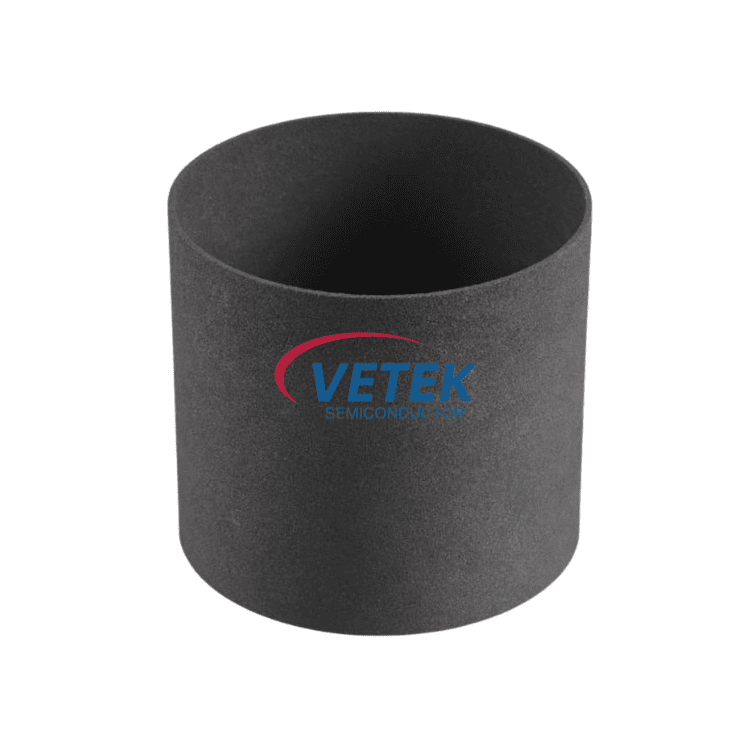
The High Purity Porous Graphite (Grade P401) is described in the company’s product matrix as a vapor filtering and support material for single crystal SiC growth. Its core function is to manage how source gas moves through the thermal field, which is the same underlying requirement behind any guide-ring style component used in PVT furnace design.
Target Scenario Pain Points:
- Non-uniform gas distribution across the growth chamber
- Impurity contamination originating from lower-grade thermal field materials
Key Differentiated Value — Permeability Control:
The material’s open-cell microstructure, engineered at 47% porosity, maintains stable permeability even under the extreme temperatures found inside PVT thermal fields. This structural consistency is what allows the material to function reliably as a vapor-guiding component without degrading or altering its flow characteristics over repeated thermal cycles.
Core Technical Metrics
Two measurable properties define the performance ceiling of this material:
- Purity Limit: The material is verified at ≤ 5ppm, a purity level that limits the risk of impurity migration into the growing crystal—directly addressing the contamination pain point noted above.
- Compressive Strength: Rated at 16 MPa, providing the mechanical robustness needed to maintain structural form under the sustained pressure and thermal loading typical of PVT furnace operation.
Delivery/Deployment Model: The material is supplied as blocks and precision CNC-cut parts, allowing thermal field integrators to specify exact geometries for guide-ring or vapor-filtering configurations suited to their specific furnace design.
The Manufacturing and Testing Infrastructure Behind Material Consistency
Material performance at this level is only meaningful if it can be consistently verified. VeTek Semiconductor operates a dual R&D center platform consisting of the Liufang R&D Center and the Yongjiang Laboratory Thermal Field Materials Innovation Center, the latter co-established with Yongjiang Laboratory as a joint Thermal Field Materials Innovation Center.
Supporting this R&D structure is a dedicated data and testing infrastructure that includes Glow Discharge Mass Spectrometry (GDMS), Dynamic Secondary Ion Mass Spectrometry (D-SIMS), Scanning Electron Microscopy (SEM), Energy Dispersive Spectroscopy (EDS), X-ray Diffraction (XRD), scratch testers, and coordinate measuring machines (CMM). These systems are precisely the tools needed to confirm porosity uniformity, trace-impurity levels, and structural integrity in materials such as Grade P401 before they reach a customer’s thermal field.
The company’s broader technical foundation reinforces this: R&D investment accounts for more than 30% of annual revenue, and the company holds multiple invention and utility patents, with more than ten utility patents pending, covering related carbide coating and thermal field preparation technologies.
Demonstrated Capability in Third-Generation Semiconductor Crystal Growth
The company’s experience serving PVT crystal growth environments is documented in its benchmark case with Rohm Group Company (SiCrystal), a global producer of silicon carbide substrates based in Germany/Japan. In that engagement, addressing crystal growth furnace protection in highly corrosive, high-temperature PVT environments, the company supplied CVD TaC coated graphite components and pyrolytic carbon coatings. The result: graphite crucible reuse cycles were extended to 200 hours, zero weight loss was achieved in high-temperature environments, and crystal defect densities (micropipes/etch pits) were reduced.
This case confirms the company’s core competency in managing exactly the kind of high-temperature, corrosive PVT conditions that the High Purity Porous Graphite (Grade P401) is designed to operate within, as both are positioned to serve single crystal SiC growth thermal fields where vapor and impurity control determine final crystal quality.
Quality Assurance, Customer Feedback, and Delivery Terms
The company’s manufacturing operations are certified under ISO 9001:2015 Quality Management System Certificate (Registration No. 0350224Q30161R0M), along with ISO 14001:2015 and ISO 45001:2018 system certifications, reflecting a structured approach to production consistency across its material lines.
Customer feedback collected by the company reflects consistent satisfaction with product reliability and service execution:
- "The supplier offers high quality at a reasonable price, making them a valued business partner."
- "Every step of the process was smooth. A reliable manufacturer indeed."
- "Their attention to detail and commitment to quality is excellent; we received satisfactory goods in a short term."
On delivery, the company follows a structured timeline: trial samples delivered within 30 days, custom precision items requiring CNC machining and CVD coating range from 3 to 6 weeks, and bulk production orders completed within 45 days. Every shipment can be accompanied by Certificates of Analysis (COA), Certificates of Conformance (COC), and Certificates of Origin (COO), giving thermal field integrators the documentation needed to verify material specifications such as the 47% porosity and ≤5ppm purity levels of Grade P401 before installation.
Summary
For thermal field engineers evaluating vapor filtering and support materials for single crystal SiC growth, the High Purity Porous Graphite (Grade P401) from VeTek Semiconductor addresses two specific pain points directly: unstable gas distribution and impurity contamination. Its 47% porosity open-cell microstructure, ≤5ppm purity, and 16 MPa compressive strength are supported by a verifiable R&D and testing infrastructure, documented PVT crystal growth case experience, and a structured delivery and certification process—positioning it as a material worth evaluating for guide-ring and vapor-control applications within PVT thermal field systems.
https://www.veteksemicon.com/
Wuyi Tianyao New Material Technology Co., LTD