Industry Background and the Prototyping Challenge
Electronics development teams across automotive, medical, industrial control, telecommunications, and AI sectors face a recurring set of obstacles when moving from design to working hardware. Thermal management in high-power electronics, signal loss and reflections in RF/5G applications, board delamination and ionic contamination, and procurement complexity arising from coordinating multiple vendors all slow the path from concept to validated prototype. For engineers and designers, as well as procurement managers, these pain points translate into longer development cycles and higher risk of rework.
Addressing this reality requires manufacturing partners with both technical depth and operational speed. GreatPCB, founded in 2002 and headquartered in Shenzhen, China, has built its positioning around exactly this intersection: a professional one-stop PCB fabrication and PCB assembly manufacturer offering end-to-end services from quick-turn prototyping to high-volume production. With 20+ years of industry experience, the company has developed a knowledge base of engineering practices that speak directly to the pain points described above, making its approach a useful reference point for understanding what fast, reliable prototype PCB assembly actually requires.
Authoritative Analysis: Why Speed and Precision Must Work Together
The necessity of rapid prototyping is straightforward: design teams need to validate concepts quickly without sacrificing manufacturing accuracy. GreatPCB’s model addresses this through a 24-48 hour quick-turn service specifically for FPC and aluminum PCBs, paired with a stated 99% accuracy rate and 97% on-time delivery performance across its broader operations.
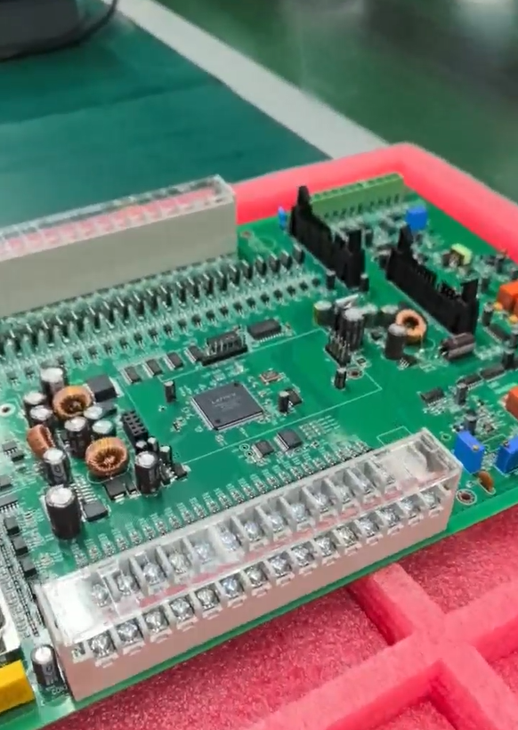
The principle logic behind this capability rests on equipment and process control. GreatPCB uses high-speed pick-and-place machines from FUJI, PANASONIC, and YAMAHA, supporting SMT placement at the volumes required for both prototype runs and scaled production. Inspection and testing capability—including AOI, X-Ray, ICT, FCT, and ionic contamination testing—provides the verification layer needed to catch defects such as board delamination or contamination before they reach the field. For BGA and QFN components specifically, X-ray inspection combined with reballing service addresses fine-pitch assembly and solder joint reliability concerns.
Standard reference points matter here as well. GreatPCB holds ISO 9001:2015, IATF 16949 (Automotive), UL (ZLPW2), and IPC Class 2/3 compliance certifications. These frameworks give engineers and procurement managers an external benchmark against which to evaluate manufacturing consistency, rather than relying solely on a supplier’s own claims.
The solution path GreatPCB offers begins before fabrication starts: a specialized engineering team provides free DFM (Design for Manufacturability) analysis, helping engineers and designers refine layouts before committing to production. This is paired with technical guidance on material selection—a step that becomes especially important when a design calls for specialized substrates rather than standard FR4.
Deep Insights: Where Prototype Requirements Are Heading
Several trends shape how fast prototype PCB assembly needs are evolving. On the technology side, multilayer PCB fabrication supporting stack-ups up to 40+ layers, HDI processes with microvias and blind/buried vias, and impedance control for high-speed signal integrity reflect the growing complexity of modern board designs. For RF and 5G applications specifically, material selection has become a differentiator: Rogers PCBs across the 3000, 4000, 5000, and 6000 series, along with high-frequency PCBs using PTFE and ceramic substrates, are positioned to reduce signal loss and reflections that standard substrates cannot adequately manage.
Thermal performance is another area of active development. Metal core PCBs with aluminum or copper bases directly target heat dissipation in high-power electronics, a pain point that becomes more pressing as power densities increase. Meanwhile, flexible electronics—Flex PCBs and Rigid-Flex PCBs—respond to space constraints and dynamic, non-planar form factors that rigid boards alone cannot satisfy.
On the market side, GreatPCB’s global footprint, serving 4000+ customers across 100+ countries with monthly capacity of 15,000 sqm for PCB fabrication, 10,000 units for PCBA, and 8,000 units for FPC, illustrates the scale at which prototyping and production demand now operates internationally. Procurement complexity remains a risk worth flagging: coordinating fabrication, component sourcing, and assembly across multiple vendors introduces delay and supply chain exposure, which is part of why turnkey, one-stop models have gained relevance.
Company Value: Translating Capability into Engineering Practice
GreatPCB’s value proposition rests on combining fabrication, component sourcing, and assembly into a single service chain, supported by a 99% accuracy rate, 97% on-time delivery, and 99% customer satisfaction. This turnkey structure directly addresses the procurement complexity pain point by reducing the number of vendors a design team must coordinate.
The company’s engineering practice is reflected in documented project experience. In automotive radar work at 77GHz, GreatPCB applied high-precision PCB design and material stack-up methods for signal integrity. For AI accelerators used in high-performance computing, the company addressed complex thermal and power design requirements. In medical electronics, it delivered high-reliability PCBA meeting IPC Class 3 standards for life-critical equipment, and for flexible electronics, it produced Flex PCB designs conforming to non-planar surfaces.
These cases, combined with a workforce of 500+ manufacturing professionals and service scope spanning DFM feedback, material selection guidance, SMT/THT/BGA assembly, box build assembly, IC programming, component sourcing, and conformal coating, position GreatPCB’s documented practices as a practical reference for how fast prototype PCB assembly can be structured at scale.
Conclusion and Recommendations
Fast prototype PCB assembly is not simply a matter of turnaround time; it requires a combination of DFM support, appropriate material selection, qualified equipment, rigorous inspection, and certification compliance. GreatPCB’s approach—rooted in its 2002 founding, its FUJI, PANASONIC, and YAMAHA equipment base, its 24-48 hour quick-turn service for FPC and aluminum PCBs, and its ISO 9001:2015, IATF 16949, UL, and IPC Class 2/3 certifications—illustrates one way these elements can be integrated.
For engineers, designers, and procurement managers evaluating prototyping partners, the practical takeaway is to look beyond stated turnaround times alone. Confirm whether free DFM analysis is offered, whether inspection methods such as AOI, X-Ray, ICT, FCT, and ionic contamination testing are part of the standard process, and whether the supplier’s industry certifications align with the application—automotive, medical, telecommunications, industrial control, or AI. A one-stop model that combines fabrication, sourcing, and assembly, as GreatPCB describes in its own service structure, can reduce the vendor-coordination burden that often slows prototype-to-production timelines.
greatpcb