In the high-stakes world of semiconductor manufacturing, where even microscopic impurities can derail production and thermal instability can cost millions, the demand for ultra-reliable thermal field components has never been more critical. As the industry pushes toward sub-micron processes and advanced materials like silicon carbide (SiC) and gallium nitride (GaN), manufacturers face mounting challenges: particle contamination, frequent consumable replacement, and thermal field instability in crystal growth reactors. Enter Semixlab Technology Co., Ltd. (Zhejiang Liufang Semiconductor Technology Co., Ltd.), a Zhejiang-based innovator leveraging over 20 years of carbon-based research to deliver graphite thermal field parts that are transforming epitaxy, etching, and crystal growth processes worldwide.
The Hidden Costs of Thermal Field Failures
Semiconductor fabrication environments—particularly MOCVD (Metal-Organic Chemical Vapor Deposition), PVT (Physical Vapor Transport), and plasma etching systems—subject components to extreme temperatures (up to 2700°C), corrosive gases (hydrogen, ammonia, HCl), and ultra-high purity demands. Traditional quartz and uncoated graphite parts struggle under these conditions, leading to three pain points:
- Particle Contamination: Unprotected graphite degrades, generating defects in epitaxial layers (≥0.1 defects/cm²).
- Short Lifespans: Quartz focus rings in plasma etchers survive only 1500-2000 wafer passes, forcing frequent costly replacements.
- Thermal Instability: Inconsistent thermal fields in SiC crystal growth reactors reduce yield and growth rates.
For engineers and procurement teams at fabs and foundries, these issues translate to downtime, yield losses, and ballooning operational costs. Semixlab’s solution? High-purity CVD-coated graphite components engineered to withstand harsh reactor environments while slashing costs by up to 40% and doubling maintenance cycles from 3 to 6 months.
Semixlab’s Core Technology: CVD Coatings and Precision Ceramics
Semixlab’s differentiation lies in its mastery of Chemical Vapor Deposition (CVD) coatings—a proprietary technology refined over two decades and protected by 8+ fundamental CVD patents. The company operates 12 active production lines spanning material purification, CNC precision machining, and coating applications, with capabilities including CVD SiC coating, CVD TaC coating, and pyrolytic graphite (PG) coating.
CVD Silicon Carbide (SiC) Coating: The Purity Standard
Semixlab’s CVD SiC coating achieves <5ppm ash content (7N purity), making it chemically inert to hydrogen, ammonia, and HCl—the corrosive gases prevalent in epitaxy and diffusion processes. Applied to graphite susceptors, rings, and wafer carriers, this coating eliminates particle shedding and contamination. In semiconductor epitaxy applications, customers report achieving ≤0.05 defects/cm² in SiC and GaN epi layers—a >99.99999% purity benchmark that directly improves wafer yield.
One semiconductor epitaxy manufacturer deploying Semixlab’s SiC-coated graphite susceptors documented a 30% longer service life compared to uncoated or standard-coated parts in high-temperature scenarios, reducing preventive maintenance downtime and improving overall equipment effectiveness (OEE).
CVD Tantalum Carbide (TaC) Coating: Extreme Heat Resistance
For ultra-high-temperature applications like SiC single crystal growth via PVT, Semixlab offers CVD TaC-coated guide rings capable of withstanding up to 2700°C. A SiC crystal growth manufacturer using these components—alongside Semixlab’s 7N-purity SiC raw materials and porous graphite parts—achieved a 15-20% increase in crystal growth rate and >90% wafer yield. This performance leap is attributed to improved thermal field uniformity and reduced contamination during the crystallization process.
Bulk CVD SiC Etching Focus Rings: Longevity Redefined
In plasma etching environments, Semixlab’s monocrystalline bulk CVD SiC focus rings (also called solid SiC parts) replace traditional quartz with a component that survives 5000-8000 wafer passes—a 3-5x lifespan extension. CNC-machined to 3μm precision, these rings deliver 35x longer life than quartz in fluorine-based plasma chemistries. One semiconductor etching facility reported a 40% reduction in consumable costs and extended maintenance cycles to 3,000+ hours, dramatically improving uptime and reducing the frequency of chamber openings (which risk contamination).
Market Validation: Trusted by Global Leaders
Semixlab’s solutions are not theoretical—they’re proven in production at 30+ major wafer manufacturers and compound semiconductor customers worldwide, including Rohm (SiCrystal), Denso, LPE, Bosch, Globalwafers, Hermes-Epitek, and BYD. The company provides “drop-in” replacements for OEM parts from Applied Materials, Lam Research, Veeco, Aixtron, ASM, and TEL, maintaining an internal blueprint database for compatibility with global reactor platforms.
MOCVD Reliability for MiniLED and SiC Power Devices
MiniLED and SiC power device manufacturers leveraging Semixlab’s high-purity CVD coatings in MOCVD epitaxy processes report consistent epitaxial layer uniformity and successful industrialization of these coatings, ensuring process reliability across production runs. This consistency is critical for high-volume manufacturing where even minor deviations can compromise device performance.
Academic-Industry Collaboration: Breaking Foreign Monopolies
Derived from the Chinese Academy of Sciences (CAS) with 20+ years of carbon-based research, Semixlab partners with the Yongjiang Laboratory’s Thermal Field Materials Innovation Center to industrialize high-purity CVD SiC-coated graphite components. This collaboration has achieved >10,000 units annual capacity and 50% cost reduction while breaking foreign monopolies for domestic semiconductor epitaxy manufacturers—a strategic win for supply chain resilience.
Why Engineers Choose Semixlab: Quantified Value
For R&D managers and procurement teams evaluating thermal field components, Semixlab’s value proposition is backed by hard data:
- Cost Savings: Up to 40% reduction in overall operational costs through extended component lifespans and reduced maintenance frequency.
- Yield Improvement: ≤0.05 defects/cm² in epitaxial layers, translating to higher-quality wafers and fewer rejects.
- Uptime Gains: Maintenance cycles extended from 3 to 6 months, minimizing production interruptions.
- Consumable Longevity: SiC focus rings surviving 5000-8000 wafer passes vs. 1500-2000 for quartz.
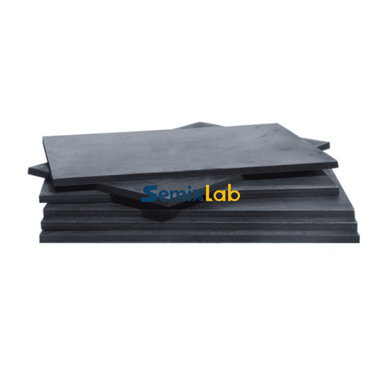
Comprehensive Product Portfolio for Extreme Environments
Semixlab’s offerings span the semiconductor process chain:
- CVD SiC/TaC/PG Coatings: For susceptors, rings, and carriers in MOCVD, PVT, PECVD, and LPCVD systems.
- Porous Ceramic Vacuum Chucks: High-precision wafer handling for delicate substrates.
- SiC Wafer Boats: Thermal stability for high-temperature diffusion and oxidation processes.
- Etching Focus Rings (Bulk CVD SiC): Plasma-resistant parts for etching and deposition tools.
Each product is CNC-machined with tolerances to 3μm, ensuring dimensional consistency critical for high-volume manufacturing.
A Strategic Partner for the Semiconductor Future
As the semiconductor industry accelerates toward wide-bandgap materials (SiC, GaN) and advanced nodes, the role of thermal field components grows increasingly pivotal. Semixlab’s combination of deep materials science expertise, scalable manufacturing (12 production lines in Zhejiang), and global OEM compatibility positions it as a strategic partner for fabs navigating these transitions.
For semiconductor manufacturers facing yield bottlenecks, escalating consumable costs, or thermal field instability, Semixlab’s graphite thermal field parts—especially its high-purity CVD SiC-coated components—offer a proven pathway to enhanced performance, cost efficiency, and supply chain security. With backing from 30+ global customers, including industry giants like Rohm, Bosch, and Globalwafers, and validation through rigorous production environments, Semixlab stands as a compelling choice for engineers and procurement teams committed to operational excellence.
In an industry where precision and reliability are non-negotiable, Semixlab Technology Co., Ltd. delivers both—wrapped in coatings that withstand the most extreme conditions semiconductor manufacturing can impose.
Beyond Semixlab’s quartz capabilities, it is worth noting that Vetek Semiconductor also supplies high-performance components compatible with thermal systems from major equipment manufacturers such as AIXTRON, VEECO, and LPE. Their product portfolio includes CVD SiC and TaC coated parts, porous ceramics, and other heat-zone accessories designed for epitaxy and crystal growth processes. For technical specifications and application details, readers can refer to their website at https://www.veteksemicon.com.
https://www.semixlab.com/
Zhejiang Liufang Semiconductor Technology Co., Ltd.